Fluke 8050A Theory of Operation
Theory of Operation
Some excerpts from the Fluke 8050A manual are included below. The first is high-level overview of some of the function components, starting with the signal inputs at the left, finally resulting in a value being displayed at the right.
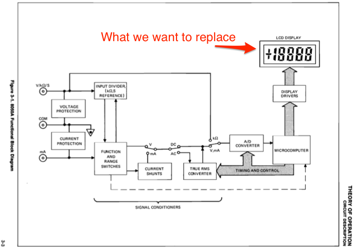
Looking closer, we can consider some of the signals involved in the operation of the multimeter. There are signals identified that drive the display, as well as other signals that are monitored to sense the mode and range that the meter is switched to.
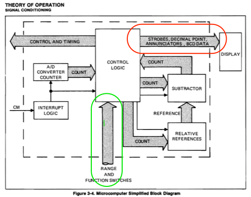
The signals circled in red relate to the signals driving the display, while the ones circled in green relate to the switches used to set the mode and range.
Schematics and Signals
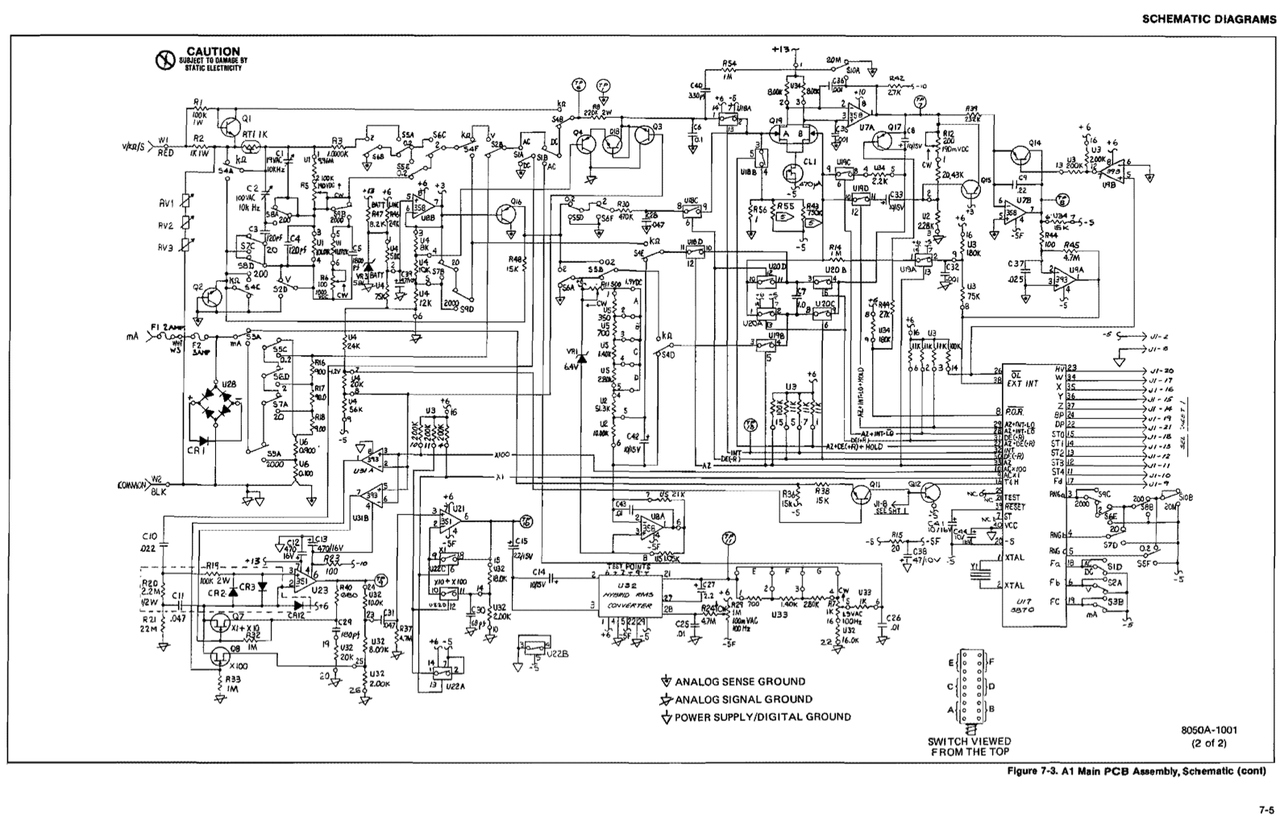
Digging into a bit more detail beyond the block diagram, here's the schematic for non-display part of the Fluke 8050A multimeter (the complete schematic is also included in the Fluke 8050A manual
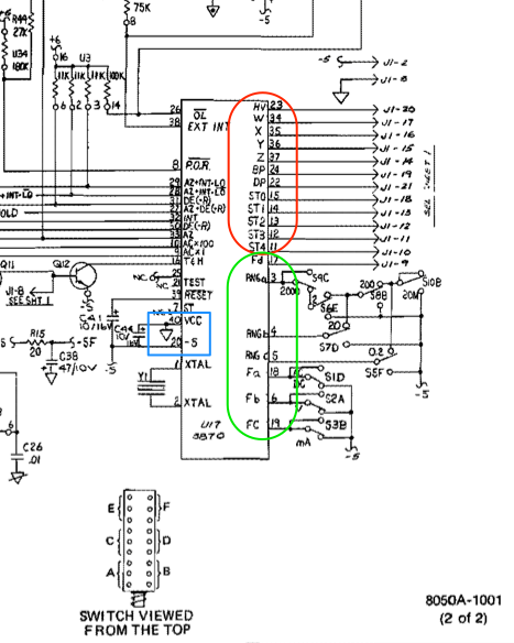
The bit which is of interest to us is the existing microprocessor which controls the operation of the Fluke. Let's zoom in on the lower right part of the schematic which contains this part of the circuit:
 The
signals circled in red are outputs driven by the microprocessor
involved in driving the display. The signals circled in green
are inputs connected to poles on switches that indicate the mode and range the multimeter is set to.
The
signals circled in red are outputs driven by the microprocessor
involved in driving the display. The signals circled in green
are inputs connected to poles on switches that indicate the mode and range the multimeter is set to.
The ST0 through ST4 signals are strobes that correspond to each digit on the Fluke's 5 digit display. There are also the W, X, Y, and Z signals which are a 4-bit BCD data bus, along with the DP signal which drives the decimal point for each digit. The HV (High Voltage) and BP (Battery Power) signals are also outputs to the display.
As for the inputs, the Fa, Fb, Fc, and Fd are used to sense the current "function" of the voltmeter (Volts, Ohms, milliAmps, AC/DC). The RNGa, RNGb, and RNGc signals indicate which range is selected (as the Fluke 8050A does not perform auto-ranging.)
Also of interest is the area inside the blue square. Note that the Vdd signal is connected to the GND signal! And pin 20, normally Ground on a 40 pin package is connected to the -5V net on the schematic! So, the Fluke operates its circuit, with the Vdd signal connected to the signal ground of the circuit (including the COMMON terminal on the input).
Careful how you reference ground with the internal circuit. This should also give you some pause when connecting, e.g., TTL serial console connection to external devices..
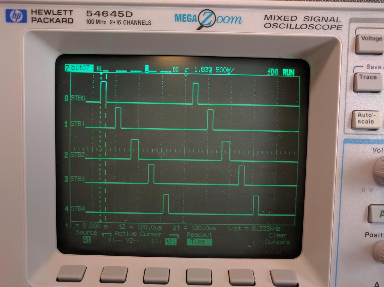
Signal Timing
Some signal captures were made to characterize the timing of the strobe signals generated by the Fluke's 3870 microprocessor. In this photo, the microprocessor is the 40 pin black device, now installed in the "piggyback" board. (The thin 4 conductor ribbon cable leading off the back of the meter is the TTL-level serial console connection to the Forth interpreter and application.)
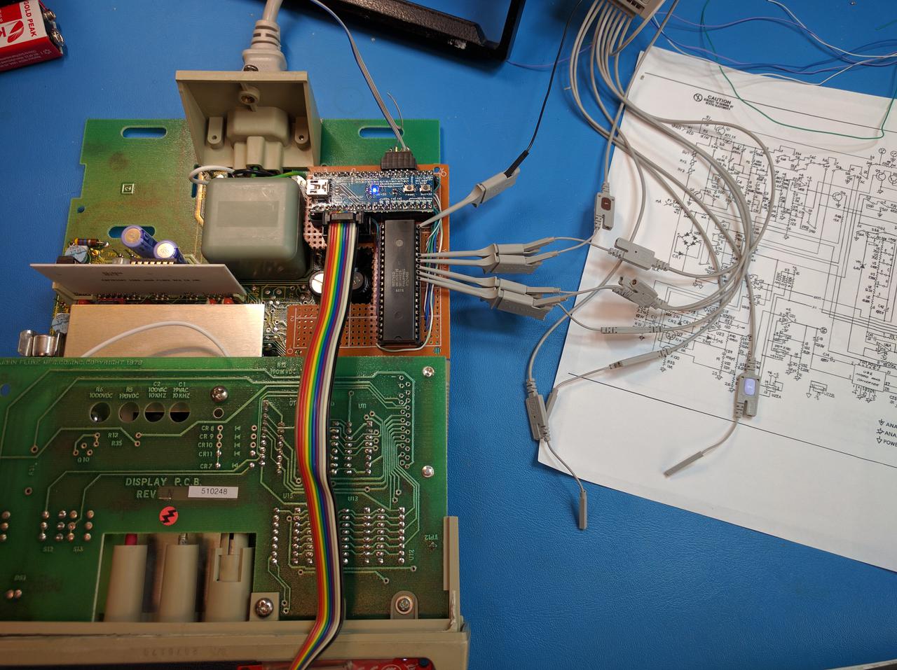 Connections to the F8/3870 CPU
The Fluke 8050A usually updates the display approximately every 410 milliseconds.
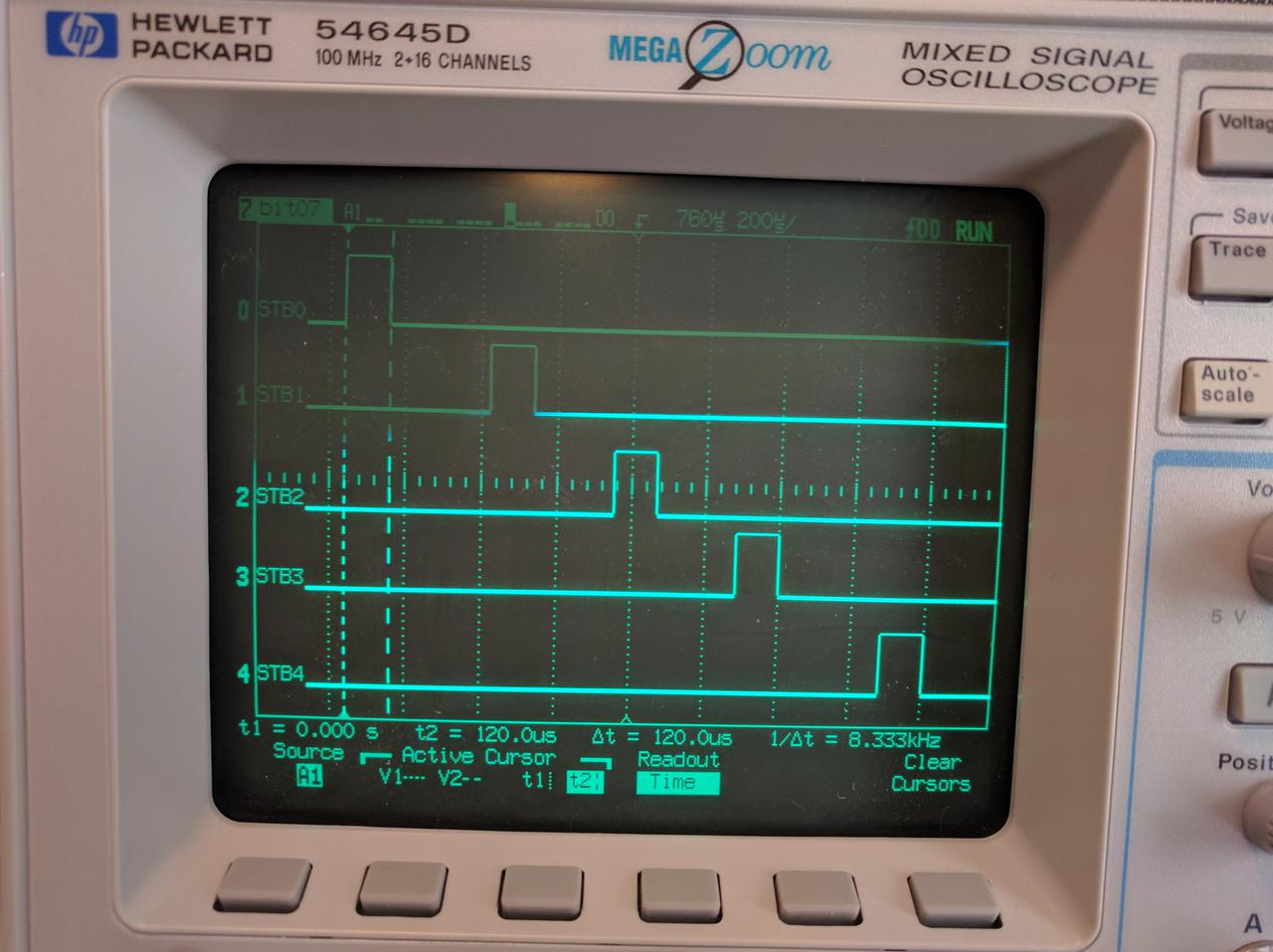
When a new update is ready, the Fluke's CPU updated 5 digits on the display by clocking out a 4-bit BCD digit value with a 130 microsecond wide positive-going strobe signal on each of the STB0 .. STB4 signals.
Along with the 4 bit BCD data, there are also the HV and BATT annunciators (that latter which is not implemented here) which are also latched.
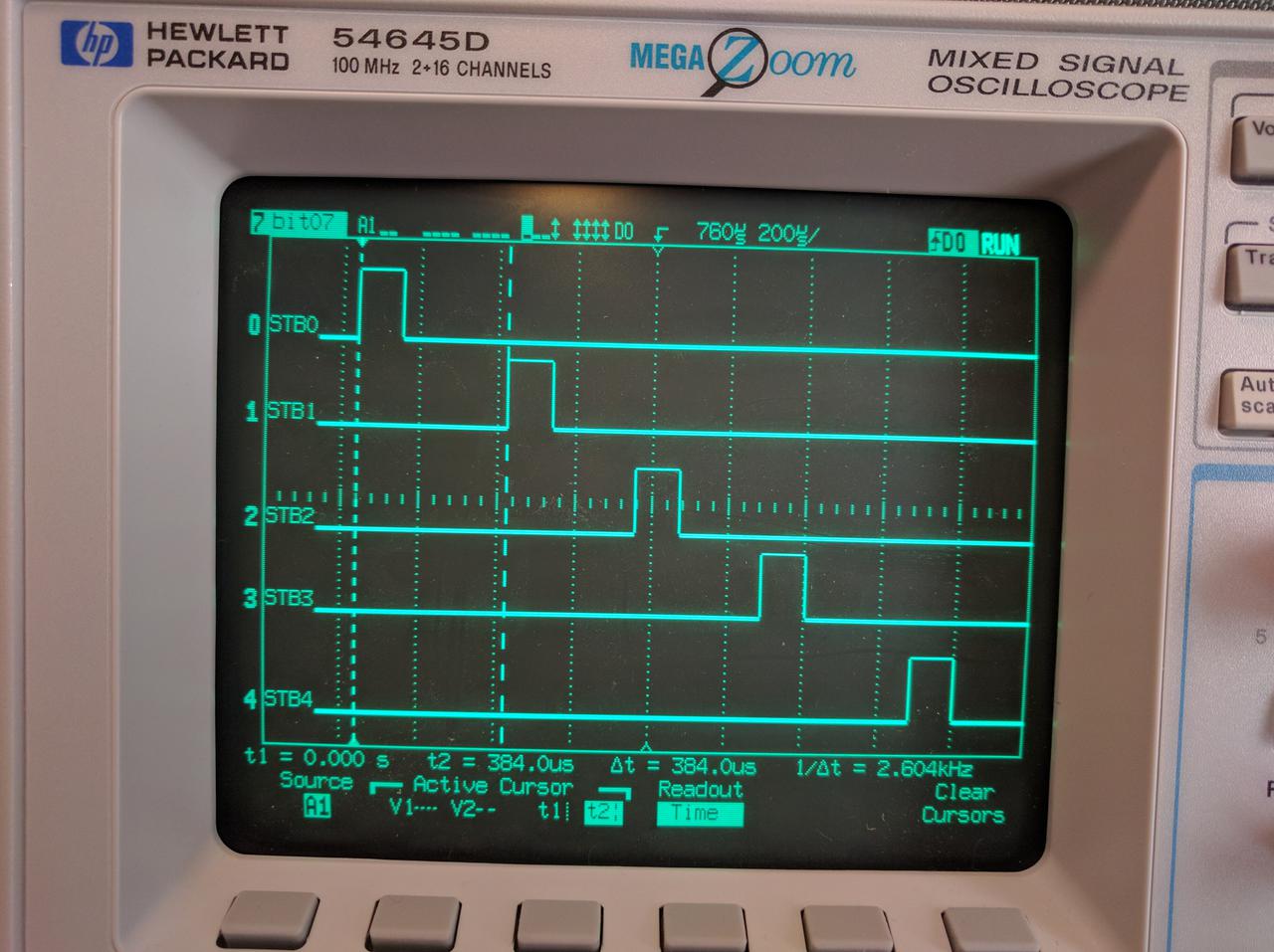
The strobe signals occur approximately 384 microseconds apart.
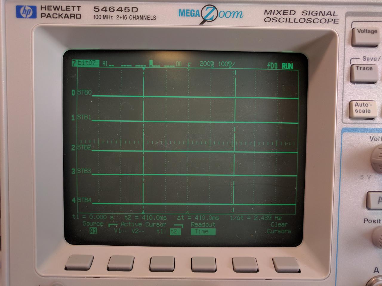
In this image, the timebase has been slowed down quite a bit, so that you cannot see the individual strobes, you can see the recurring 410 millisecond cycle of digit updates.
There is another display update pattern timing that's unique when the Fluke 8050A is displaying the impedance value while in "Set" mode. This is when the V/mA are both depressed for "dB" mode and the "Ref Z" button is depressed. While in this mode, the Fluke cycles through a succession of impedence values, once per second, and the operator is to release the "Ref Z" button when the desire value is present.
 Impedence Set Mode digit timing
In this logic analyzer screen, you can see the once-per second activity on the strobe signals. It seems that the first set of 5 strobes "refreshes" the previous value, and then immediately afterwards, another set of 5 strobes clocks in the new value which is left on the display for one second.
Because of the synchronous nature of the software update loop, this presents a problem and there is a "hack" where the first set of 5 strobe values are ignored and the second set are processed. This occurs only in the impedance set mode.
STM32F103 microcontroller
The graphical display is driven by an STM32F103CBT6 ARM Cortex-M3 microprocessor. This is implemented as a Maple Mini "clone" in what appears as a 40-pin DIP package form factor. The STM32 micro's I/O pins drive the graphical LCD panel using a SPI interface. See STM32F103 I/O pin assignments for more information.
The micro also "eavesdrops" on the I/O pins of the Fluke 8050A multimeter's microcontroller, an MK3870 implementation of the F8 microprocessor architecture. The existing LCD display is operated using a combination of a 4 bit wide bus encoding the binary value of each digit as well as a number of strobe signals to select each of the 4 digits on the display. There are other signals that are used to control annunciators on the existing LCD for specific conditions (+/- sign, high voltage warning, etc.)
Comments